Best Universal Logic Gate Converter: Simplify Digital Design
Convert Boolean expressions to NAND/NOR, generate Verilog & VHDL, build truth tables, K-Maps, and analyze gate count — 100% offline.
Related Article Slug: universal-logic-gate-converter-guide
Table of Contents
Last updated: June 2026
🔴 The Foundational Mathematics of Digital Hardware
Designing digital circuits can be incredibly mathematically intensive without the correct methodologies and calculation resources. Whether you are an electronics engineering student studying computer architecture or a seasoned hardware designer drafting a new printed circuit board, applying a reliable gate conversion tool is an absolute necessity for streamlining your workflow. Before a computer can execute a single line of software code, a physical layer of hardware must process binary signals efficiently.
At the lowest physical level of all computing hardware lie standard logic gates. These microscopic building blocks perform the fundamental logical functions required for any digital circuit to operate. The entire concept relies heavily on Boolean algebra, a branch of discrete mathematics formulated by George Boole in the 19th century that maps logical truth values to binary ones and zeros. Standard digital hardware traditionally relies on three primary logic functions: AND, OR, and NOT. An AND gate outputs a true signal only if all of its inputs are true, mathematically expressed as Y = A · B. Conversely, an OR gate outputs a true signal if at least one of its inputs is true, denoted as Y = A + B. The NOT gate inverts the incoming electrical signal, flipping a binary 1 to 0 and vice versa. These three primitives form the foundation of every CPU, memory controller, and logic array ever manufactured.
Understanding gate behavior at this level is not optional for serious engineers. It is the bedrock. A student who cannot mentally trace a signal through cascaded gates will struggle with FPGA programming, ASIC design, and even basic PCB troubleshooting. The mathematics must become second nature before real hardware design can begin.
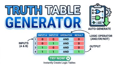
Truth tables are the primary tool for verifying gate behavior. Each row represents one possible combination of input signals, and the output column shows the resulting binary state. For a two-input AND gate, only one row — where both A and B equal 1 — produces a HIGH output. For a two-input OR gate, three out of four rows produce a HIGH output. These tables seem simple in isolation, but complex circuits combine hundreds of gates simultaneously, making manual verification practically impossible at scale.
🟡 Understanding NAND and NOR Universality
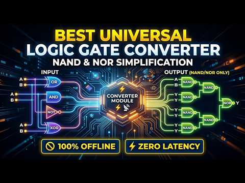
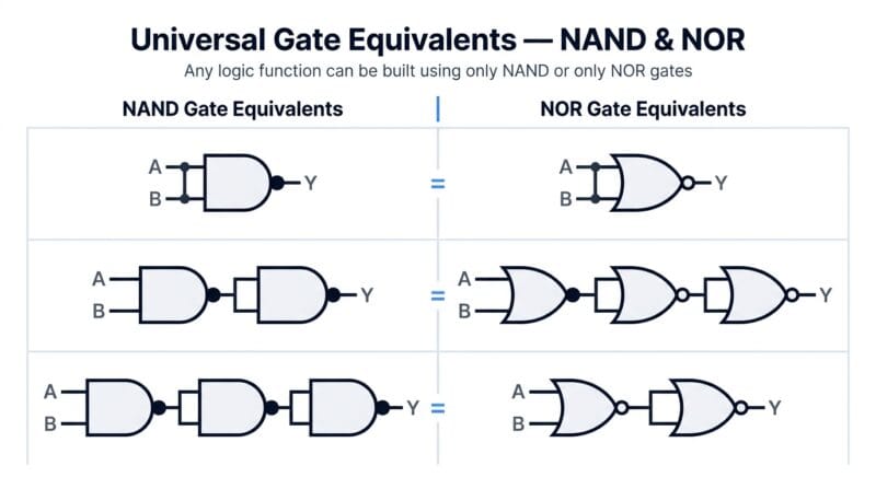
In practical hardware manufacturing, designing circuits using a mixed variety of AND, OR, and NOT chips is highly inefficient and expensive. NAND (NOT-AND) and NOR (NOT-OR) gates are uniquely classified as “universal” because a hardware designer can construct any other logical function imaginable using only these specific gate types.
Instead of buying three different types of microchips, an engineer can buy a single bulk order of NAND chips and wire them to replicate the behavior of any other gate. The economics are dramatic. The 74HC00 quad NAND package costs a fraction of purchasing separate 74HC08 AND, 74HC32 OR, and 74HC04 NOT chips — and it eliminates the supply chain complexity that plagues small production runs.
By tying the inputs of a NAND gate together, it instantly mimics the exact behavior of a NOT gate. By combining multiple NAND gates in specific cascaded arrangements, you can flawlessly replicate standard AND and OR functions, drastically reducing the unique variety of microchips needed on a motherboard. You can read more about the mathematical proofs behind this concept in the Wikipedia documentation on NAND logic.
NOR universality follows the same principle from the complementary direction. A single NOR gate with tied inputs produces a NOT function. Cascading NOR gates reconstructs OR and AND operations through sequential inversion. The choice between NAND-only and NOR-only implementations often depends on the target technology — CMOS families tend to favor NAND implementations due to slightly better propagation characteristics, while certain TTL families lean NOR.
🟢 De Morgan’s Laws and Algorithmic Translation
To fully grasp the theoretical power of these hardware transformations, engineers must study De Morgan’s Laws. These foundational rules dictate how logical statements interact with negation. The first theorem states that the complement of a product equals the sum of complements: NOT(A AND B) = NOT(A) OR NOT(B). The second theorem mirrors this: NOT(A OR B) = NOT(A) AND NOT(B). These proofs are the mathematical engine that makes universal gate conversion possible.
Manually applying De Morgan’s formulas to a circuit with dozens of variables is tedious and highly prone to human error. This is precisely where automated conversion tools save engineering hours. Applying strict computational parsing to Boolean equations eliminates transcription mistakes and produces verified equivalent circuits in milliseconds.
When you transition these concepts into real-world applications, you will discover several critical engineering advantages. A proficient gate conversion workflow provides the following practical benefits for digital logic design:
🔵 Reduces Component Count: Standardizing the logic gates across the entire board minimizes the physical footprint of your circuit, freeing PCB space for additional functionality.
🟠 Lowers Manufacturing Costs: Ordering a single type of integrated circuit (like the 7400 Quad NAND gate) in bulk is far cheaper than sourcing mixed components across multiple supplier catalogs.
🟣 Simplifies Troubleshooting: Quality assurance testing becomes much easier when engineers only have to verify one type of logic behavior across the schematic, cutting QA time significantly.
🔵 Optimizes Signal Propagation: Careful algorithmic translation ensures that signals travel through the minimum required number of transistor layers, reducing gate delay and improving clock speed margins.
Beyond cost and speed, there is a deeper benefit — design portability. A circuit expressed entirely in NAND logic can be ported to any CMOS process node without renegotiating with multiple component suppliers. The schematic becomes process-agnostic. That is a significant advantage in an industry where semiconductor supply chains can shift overnight.
For students preparing for university exams in digital electronics, mastering this conversion process manually builds the intuition required to tackle Karnaugh map minimization and sum-of-products optimization. You can deepen that foundation by reading our related article on Boolean algebra simplification techniques.
🔴 Client-Side Security and Offline Processing
Transitioning from theoretical Boolean mathematics to practical circuit deployment requires reliable software. After mastering the foundational concepts of De Morgan’s laws, the next logical step is to integrate a dedicated conversion tool into your daily engineering workflow. Data security, however, is a massive concern in the semiconductor and hardware design industry.
Many online electronics calculators process your proprietary schematics on remote cloud servers. This exposes your intellectual property and academic research to severe privacy risks. Patent-pending circuit designs, university thesis work, and proprietary ASIC layouts should never travel through a third-party server you do not control.
The universal logic gate converter provided on this platform is strictly client-side. The entire algebraic translation algorithm executes directly inside your local web browser’s memory sandbox. Your complex logic grids and hardware blueprints never leave your local machine, guaranteeing zero server latency and complete data sovereignty.
This offline-first architecture also means the tool works without an internet connection after the initial page load. No network requests are made during conversion. Engineers working in secure facilities with network-restricted environments can run full Boolean conversions without triggering any outbound data transfers. No account. No telemetry. No cloud dependency whatsoever.
Do not let complex Boolean algebra slow down your project timeline or inflate your manufacturing costs. Expand your engineering toolkit by exploring our completely secure, privacy-first software collection at the PrimeToolHub main directory. By shifting to local, client-side execution, your gate conversion workflow runs instantly, keeping proprietary circuit designs entirely in your control.