Digital Logic Studio Pro
Use Digital Logic Studio Pro to convert Boolean formulas to 7400/4000 series ICs, generate NAND/NOR universal forms and visualize SVG circuit diagrams — 100% offline.
Table of Contents
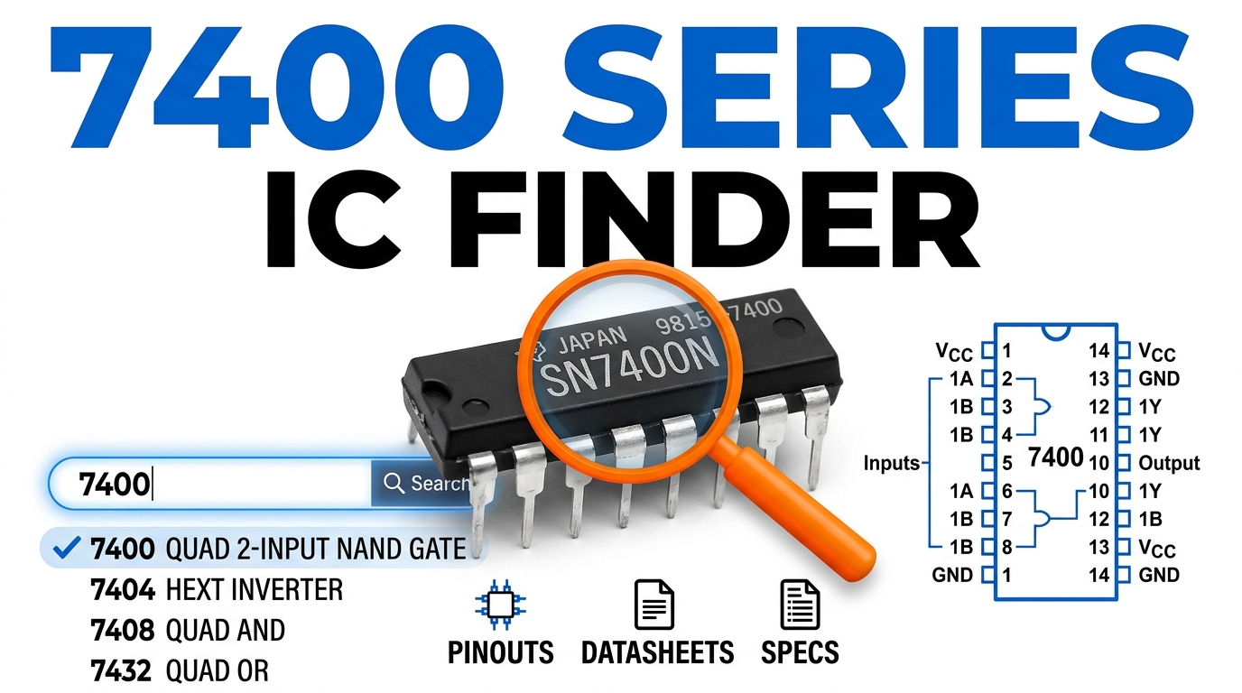
Poking through a parts drawer trying to remember what a 7400 chip actually does? Look up 7400-series ICs to find pinouts and functions, so you can match a part to your breadboard project. A quick reference for when the datasheet is not in front of you.
Digital Logic Studio Pro
Boolean to IC converter, NAND/NOR universal equivalents, SVG circuit builder, full 7400/4000 series library & Boolean laws reference. 100% offline.
📊 Need full truth table, equivalence checker or Verilog export?
Truth Table Studio Pro →🔢 Need visual K-Map minimization or Quine-McCluskey reduction?
K-Map Solver →Expression Analysis
Recommended IC
Universal Equivalents
NAND-only form:
NOR-only form:
IC Pinout Diagram
Educational pinout — always verify against the manufacturer datasheet before wiring.
ℹ️ Circuit diagram auto-updates after each Analyzer run. Enter a formula in the Analyzer tab first.
Go to Analyzer →Simplified gate-level schematic. Complex nested expressions show up to 3 gate levels.
History is stored in memory only and clears when you reload the page.
Boolean to Hardware in One Step
Type any Boolean expression — including NAND, NOR, and XOR operators — and the Analyzer tab returns the matching IC part number, gate configuration, pin package, and supply voltage for either the 7400 TTL or 4000 CMOS family. Switch families with the dropdown and the IC recommendation updates instantly without re-running anything.
35-IC Searchable Library
The IC Library tab holds 35 integrated circuits across both families — 13 TTL (7400 through 7486) and 22 CMOS (4000 through 4093). Filter by family, gate type, or search by part number to compare gate count, input count, pin package, and voltage in one place. Useful when the recommended IC is out of stock and you need a functional alternative.
Live SVG Circuit Builder
Every analysis automatically draws a live SVG gate diagram in the Circuit Builder tab. Simple expressions get a clean input-to-gate-to-output schematic; compound expressions show a hierarchical two-level layout with connecting wires. The SVG downloads to your device for use in reports, lab sheets, or slide presentations without screen-capturing.
How to Use Digital Logic Studio Pro
Enter Your Formula
Type a Boolean expression in the input box — words like AND, OR, NOT, NAND, NOR, XOR all work — or tap a Quick Load tag for an instant example. Press Enter or click Analyze.
Choose Your IC Family
Use the dropdown to select TTL 7400 (5V fixed rail) or CMOS 4000 (3-15V wide range). The IC recommendation, gate count, pin package, and pinout diagram all update to match your chosen family.
Read the Results
The Analyzer returns the readable form, symbolic notation, generator format, dominant gate type, matched IC part number, NAND-only form, and NOR-only form. Click the pinout to see pin assignments.
Explore Other Tabs
Switch to Circuit Builder for the SVG schematic, IC Library to find alternatives, Boolean Laws for the algebra reference, or History to reload any previous formula from the current session.
Last updated: July 2026
🔴 TTL or CMOS? Making the Right Call Before You Order Parts
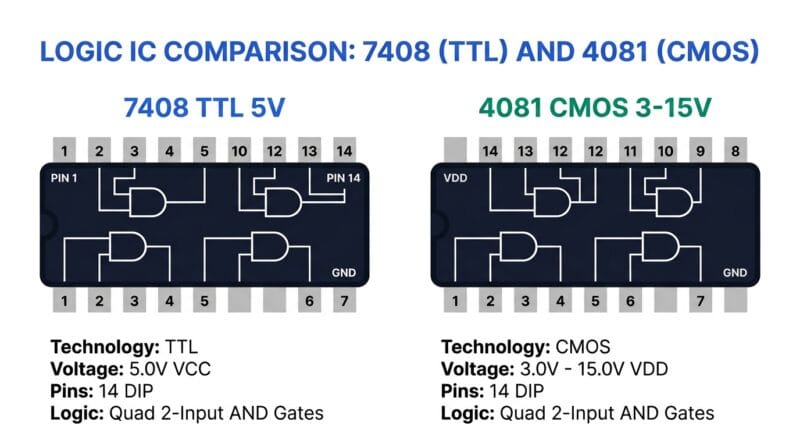
The IC family dropdown in the Analyzer tab is not just a cosmetic toggle — it changes which chip the tool recommends, and choosing wrong means the part you order will not work with the rest of your circuit. Here is the practical breakdown.
Pick TTL (7400 series) when your circuit runs on a fixed 5-volt regulated supply and you are working with classic classroom hardware, breadboard lab kits, or any project that already uses 5V logic throughout. TTL chips switch fast, are extremely well-documented, and a datasheet for the 7408 quad AND gate has not changed materially since 1972. The 7400, 7408, and 7404 are three chips every electronics bench should have in a drawer.
Pick CMOS (4000 series) when your supply voltage is anything other than a steady 5V, when the circuit runs from batteries, when power consumption matters, or when you need to interface with 3.3V microcontrollers. The 4011 (NAND) and 4071 (OR) run comfortably anywhere from 3V to 15V and draw near-zero static current. A coin-cell LED driver built around CMOS can survive weeks; the TTL equivalent would flatten the battery in hours.
One situation students regularly get wrong: mixing TTL and CMOS in the same circuit. A TTL gate output driving a CMOS input usually works, but a CMOS output at 15V driving a TTL input rated for 5V will kill the TTL chip immediately. Keep families separate unless you have a buffer IC (like the 4050) specifically designed for level shifting between them.
🟡 What the Pinout Diagram Is Actually Showing You
The Analyzer tab draws a simplified DIP (Dual Inline Package) pinout whenever an IC match is found. Reading it takes about thirty seconds once you know the convention, and it applies to almost every 7400 and 4000 series chip you will encounter.
- 🔵 The notch or dot marks pin 1 — always at the top-left when the chip is oriented with the notch facing toward you.
- 🟠 Pins number counter-clockwise around the package: down the left side, then up the right side.
- 🟣 The bottom-left pin is always GND (ground). The top-right pin is always VCC (positive supply). These are the same on almost every 14-pin DIP logic chip.
For the quad 2-input AND (7408), pins 1-2 are the two inputs to gate 1, pin 3 is gate 1’s output, pins 4-5 are gate 2’s inputs, pin 6 is gate 2’s output — and the same pattern repeats for gates 3 and 4 on the opposite side of the chip. Once you see this layout on the 7408, you will immediately recognize the same four-gate arrangement on the 7400, 7402, 7432, and 7486. The pinout diagram here is for orientation — always pull the manufacturer’s datasheet before soldering a physical board.
🟢 Why NAND and NOR Conversions Appear on Every Analyzer Result
Every Analyzer result includes both a NAND-only and a NOR-only form of your expression. This is not just academic — it is genuinely useful in three real situations.
Single-chip builds: If you need both an AND function and an OR function but only want to order one chip type, you can implement both using NAND gates from a single 7400. The NAND conversion tells you exactly what to wire. For (A AND B): connect the NAND output back to itself as a second input to get NOT(NAND), which equals AND. It takes one extra gate but keeps your BOM (bill of materials) to one line item.
Exam verification: A common digital logic exam question asks you to prove De Morgan’s theorem by implementing NOT(A AND B) using only NOR gates. The NOR-only conversion in the tool shows the answer immediately, but more importantly shows the structure — which helps when the exam asks you to draw the gates, not just write the expression.
FPGA synthesis: Modern FPGA tools convert all logic to NAND-NAND or NOR-NOR networks during technology mapping because CMOS transistor pairs implement NAND naturally. Understanding what the tool generates here gives you a window into what your synthesis tool is doing under the hood. For a deeper step-by-step simplification, take the expression to the Boolean Expression Simplifier to see each Boolean law applied in sequence.
🔴 Reading the Circuit Builder Diagram
Simple formulas — a single AND, OR, NOT, or one-level compound expression — produce a clean schematic: inputs on the left, a labeled gate rectangle in the middle, and the output labeled Y on the right. Connecting wires run left to right and meet at the gate inputs.
For two-level expressions like (A AND B) OR C, the diagram adds a second column: all leaf terms fan into the center gate, which feeds the output. The more complex the expression, the deeper the hierarchy. Formulas with more than three levels of nesting show a simplified summary view noting the root gate type and expression depth — at that point, the full schematic is impractical to read in a browser window, and you would normally use a dedicated EDA (Electronic Design Automation) tool to generate the full net list. Download the SVG using the button below the diagram to embed it directly into a lab report or slideshow without re-screenshotting every time the formula changes.
For truth table analysis, equivalence checking, or generating Verilog HDL from your expression, use the Truth Table Studio Pro. For visual K-map grouping and Quine-McCluskey minimization, the K-Map Solver Pro handles 2 to 5 variables with prime implicant visualization.
🟡 Getting the Most from the IC Library Tab
The IC Library lists 35 chips across both families, filterable by gate type and searchable by part number or description. A few practical uses:
- 🔵 Finding a 3-input alternative: The Analyzer recommends the 2-input variant for most formulas. If your design actually has three inputs to a single AND gate, filter by “AND” and look for the 7411 (TTL) or 4073 (CMOS) — both are triple 3-input AND chips.
- 🟠 Sourcing a substitute: The 4069 and 4049 both invert — but the 4049 is rated for level-shifting from higher voltages down to 5V, while the 4069 is a standard-rail inverter. If your distributor is out of the 4049, the library description flags this distinction clearly.
- 🟣 Comparing gate density: The 7430 fits a full 8-input NAND gate in a single 14-pin DIP package. If your address decoder uses an 8-line AND, one 7430 replaces what would otherwise require three cascaded 7408 chips. Search “8” in the library to pull it up immediately.
What’s the difference between the 7400 and 4011 NAND chips?
Both contain four 2-input NAND gates in a 14-pin DIP package — they are functionally identical in logic. The 7400 is TTL, running only on 5V with fast switching. The 4011 is CMOS, running on 3V to 15V with far lower power draw. Use the dropdown to switch between them and the pinout redraws.
Why does the tool always show NAND and NOR forms even for simple AND formulas?
Because NAND and NOR are universal — any gate can be built from them. The conversions appear every time because the most common reason engineers want them is precisely for simple expressions where they want to consolidate to one chip type. Complex formulas make this obvious; simple ones are where it saves the most board space.
Can I paste the generator format directly into another tool?
Yes. The generator format is a lowercase version of your expression using words (and, or, not) rather than symbols, compatible with Boolean expression parsers, simulation tools, and the Boolean Expression Simplifier on this site. Copy it with one click from the Analyzer tab.
The recommended IC has 4 gates per package but I only need 1. Is that a problem?
Not at all — this is normal for DIP logic ICs. Just leave the unused gate inputs tied to a defined logic level (GND for CMOS NAND, VCC for CMOS NOR) rather than floating. A floating input on a CMOS chip picks up noise and can oscillate unpredictably.
Where can I verify truth table outputs for a formula I analyzed here?
Take the expression straight to the Truth Table Studio Pro. It evaluates every input combination, shows intermediate sub-expression columns, and generates Verilog HDL you can load into DigitalJS to watch the gates toggle in real time.
How do I find a 3-input OR gate in the IC Library?
Open the IC Library tab, set the gate type filter to OR, and look for the 4075 (CMOS triple 3-input OR). There is no 7400-series 3-input OR with four gates in one package — the closest is the 7432 (2-input), so for 3-input OR you would cascade two 7432 gates or switch to CMOS.
Does the SVG circuit diagram update automatically?
Yes. Every time you run an analysis in the Analyzer tab, the Circuit Builder tab regenerates the SVG immediately. Switch tabs and it is already there — no separate button to press. If the expression is deeply nested, the diagram shows a simplified summary view with the root gate and expression depth labeled.
What is the 4093 in the CMOS library and when would I use it?
The 4093 is a quad 2-input Schmitt-trigger NAND. A Schmitt trigger adds hysteresis — the switching threshold for a rising signal is higher than for a falling one. This makes it ideal for cleaning up slow or noisy signals like those from RC circuits, push buttons, and capacitive sensors, where a standard NAND would oscillate at the threshold.